

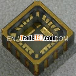
Description:
1.Inner Layer Milling Technology 2.Patent approved 3.Gold plating4.Glass EpoxyInner Layer MillingTechnology(Patented)
Our original inner Layer millingtechnology makes possible to accurately expose inner layer copperpattern by detecting such copper pattern position. It enable tomake tiers width narrow due to prevention of prepreg blur onbonding pad occurring in case of stacking method. As a result, itis available for making bonding wire length short and itsconnection reliability higher and achieving compact PCB. Moreover,it enables to provide high reliability PCB and also apply toelectroless soft gold plating because of no void in boundarybetween inner layers. It is available for high-speed processing,higher yield and lower cost.
•KEY TECHNOLOGY
| FA & Robot | Automobile | Medical & Sensing | LED | Chip size Package | High Frequency Module | Chip on Board | BGA | Multi Chip Module | |
| Inner Layer Milling Technology | A | B | A | B | A | A | A | A | A |
| High Dam Printing Technology | A | B | A | B | A | A | A | A | A |
| Laser via Technology | A | B | A | B | A | A | A | A | A |
| Stacking Technology | A | B | A | A | B | A | B | A | A |
| Electroless Soft Gold plating Technology | A | A | A | A | A | A | A | A | A |
| Pin Caulking Technology | B | B | A | B | B | A | B | A | B |
| Dry Film Tent on Via Technology | B | B | B | A | A | B | A | B | B |
| Punching Technology | B | B | B | A | B | A | B | B | A |
| Flat Push Back Technology | A | A | A | A | B | A | B | B | A |
•CAPABILITIES
Panelsize = 340x340mm
406x340mm
510x340mm
Thickness = 0.06-3.0mm
Material = Hitachi, Mitsubishi,Matsushita,
Risho, Kyocera, Rogers
Capacity = 10, 000m²/month over
Products = Dual side PCB
Multi-layer PCB (3-16 layers)
Build-up PCB

