

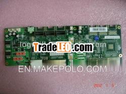
Description:
PCBA for control board Material used: FR4, High Tg Minimum 170C,Hifrequency. Layer Count: 2-12 layers Via / Drill Size:PCBA for control board
We cansupply PCBA, SMT final assembly-vertical integrated manufacturingsolution.
Capable ofdeveloping effective production
Our PCB capability:
Material used: FR4, High Tg Minimum 170C, Hifrequency, metal based: Aluminium ect.
Maximum Panel Size: 26" X 26" (660mm X 660mm)
Line Width & Spacing:
Minimum Line Width (Internal) 4 mil (0.1 mm) for mass production and 3mil for samples
Minimum Line Width (External): 4 mil (0.1 mm) for mass production and 3 mils for samples.
Minimum Line Spacing (External): 4 mil (0.1 mm) for mass production and 3 mils for samples.
Layer Count & Thickness: 2-12 layers
Minimum Thickness (2 Layers): 4 mil (0.1 mm)
Minimum Thickness (4 Layers): 12 mil (0.3 mm)
Minimum Thickness (6 Layers): 16 mil (0.4 mm)
Minimum Thickness (8 Layers): 24 mil (0.6 mm)
Maximum Thickness(10layers): 200 mil (5.0 mm)
Layer to Layer Registration: /- 5 mil (0.13 mm)
Via / Drill Size: Minimum Drill Hole Diameter 10 mil (0.25 mm)
Minimum Via Size: 8 mil (0.2 mm)
Hole to Hole Tolerance: /- 3 mil (0.08 mm)
Hole to Edge Tolerance: /- 5 mil (0.13 mm)
Micro Via: 4 mil (0.1 mm)
Solder Mask: Solder Mask Bridge Between Solder Dam 3 mil (0.07 mm)
Warpage: 0.5 %
Impedance: /- 10%
Surface Finish: Hard Gold / ENIG / HASL / Carbon Ink / OSP (ENTEK CU 106 AX) / Immersion Tin
Min. SMT Ptich: 12 mil (0.2 mm)
Min. Parts footpins: 0201
Products involved fields: Consume Electronics, Medical equipments, Industrial commands, communications, auto parts ect.
Logwell was founded in 1997, the founder Mr. Gary Hsu is in the PCindustry nearly 30 years. Starting from the era of Apple Ⅱ, Garybegan his career as an motherboard engineer, pass through the8088/x86 period. Gary has been involving in development many typeof motherboards, chipsets. With accumulated working experience,Gary earns the know-how not only in technical but also in theproduction.
Garyestablished Logwell,starting on his own development of environment chips, supplyingsolutions to other PC periphal manufacturer. As the businessexpands, Logwell starting its own assembly line production to giveproactive service, including SMT, DIP, function test and assemblyline for finish good. There are two plants, one is with totalinvolvement, the other is dedicated for assembly.
Logwell isISO9001 certified with around 130 employee include management andR&D team. The capacity build up to provide world class servicein PC, 3C industry to ODM/OEM customers. Our capabilities not onlyin production service, but also offering value added designservice, keeping our partner leading in technically, timely and thecost effective way.
1.Capacity & Staves
| Function | Position | Capacity | Shift | Manpower |
| SMT | Line 1 | 1.5M/day | Two | 28 |
| Line 2 | 500K/day | Two | ||
| Line 3 | 500K/day | Two | ||
| DIP | Line 1 | 2, 500 pcs/day | One | 18 |
| Line 2 | 2, 500 pcs/day | One | ||
| Assembly | Line 1 | One | 43 | |
| & Testing | Line 2 | One | ||
| QA | 6 | |||
| Support | 35 |
2. SMT Specialty
| PANASONIC | YAMAHA | ||
| PCBSize | Max.: | 510×460(mm2) | 450×330(mm2) |
| Min.: | 50×50(mm) | 50×50(mm) | |
| PCB Thickness | Max.: | 4mm | 3.2mm |
| Min.: | 0.3mm | 0.5mm | |
| Component Dim. | 1005 | 201 | |
| IR Reflow | N2OK | ||
| What We Had | Mother Board | ||
| Expander Board | |||
| Back PlaneBoard | |||
| FPC | |||
| Small Board | |||
| …. Etc | |||
3. Facility Reality
4.Certification
Welcome to join us !
OEM/ODM PCB Assembly Service
PCB Sample Run 1~3 Days
Powerful Components Purchasing
PCBA Engineering Run 1~3 Days
ISO9001

