

Description:
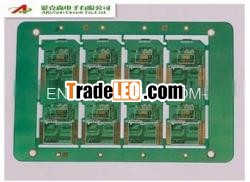
Multilayer pcb(6L) Rigid (1~30 layers), Flex (1~8 layers)Rigid-flex circuits (1~6 layers) Electronic components, PCBA, FPCAHDI Printed Circuit Board
AkesonPCB is a leading production company specialized in producing smallquantity and diverse PCB prototypes.
Wemanage fast time-to market to the standard for qualityassurance.
GeneralManufacturing Capability
Category | Description | Capability |
FileFormats | Gerber files-preferred | 274-X, 274-D,DPF, ODB |
Drillfile | X & Ycoordinates, with tool sizes included | |
Size | Max. finisheddimensions | 580mmx 800mm – Single/Double-sided |
550mmx 800mm –Multilayer | ||
BoardThickness | Standard | 1.6mm±10% |
Min. | Single/Double-sided:0.2mm ±0.1mm | |
4-layer:0.4mm±0.1mm | ||
6-layer:0.6mm±0.1mm | ||
8-Layer:1.0mm±0.1mm | ||
10-layer:1.0mm±0.12mm | ||
12-layer:1.2mm±0.12mm | ||
… | ||
32-layer:4.0mm±0.4mm and above | ||
Max. | 6.3mm±10% | |
Bow andtwist | <7/1000 | |
Copper | Outer Cuweight | 1oz~ 10oz |
Weight | Inner Cuwight | 1/3oz ~6oz |
LaminateMaterials | FR4(High TG,halogen-free), FR5, ISOLA(FR408, 370HR), TEFLON, POLYIMIDE,ROGERS(RO4003, RO4350, RO4450), Aluminum plate (Single,Double-sided) | |
FR4Thickness | 1.6mm | |
High TG FR4(170 deg C) | 1.6mm | |
BoardCutting | Max. number oflayers | 32 |
Min. thicknessfor inner layers (Cu thickness are excluded) | 0.07mm | |
Drilling | Min.size | 0.1mm |
Max.size | 6.0mm | |
DrillDeviation | ±0.002”(0.050mm) | |
PTH holetolerance | ±0.003”(0.075mm) | |
NPTH holetolerance | ±0.002”(0.050mm) | |
Angle ofCountersink | 80°, 90°,100°, 120° | |
Plating | Min. holesize | 0.0008” |
Aspectratio | 20 | |
Etching | Trace widthtolerance | ±20% |
Min. tracewidth / space (1oz finished Cu weight starting from1/3oz) | 0.003”/ 0.003”(0.08mm) | |
Min. tracewidth / space (1oz finished Cu weight starting from1/2oz) | 0.004”/ 0.004”(0.1mm) | |
Min. tracewidth / space (2oz finished Cu weight) | 0.005”/ 0.005”(0.127mm) | |
Min. tracewidth / space (3oz finished Cu weight) | 0.008”/ 0.008”(0.2mm) | |
Min. tracewidth / space (4oz finished Cu weight) | 0.012”/ 0.012” (0.3mm) | |
InnerLayers | Min. spacefrom drilling to inner pattern | 0.1mm |
Min. spacefrom annular ring to inner pattern | 0.1mm | |
Layer-to-layerregistration | ±0.003”(0.08mm) | |
SolderMask | Color | green, lightgreen, matte green, white, extreme white, black, matte black, darkbrown, yellow, red, blue, transparent |
Min. soldermask clearance | 0.003” | |
Thickness | 0.0004” | |
Silkscreen | Color | White, black,yellow, red, blue, green |
Min. tracewidth | 0.005” | |
Min.size | 0.028”/0.028” | |
ElectricalTest | AOI | Y |
Flying ProbeTester | Y | |
ControlledImpedance | Tolerance | ±10% |
Impedancetester | TektronixTDS8200 | |
Routing | End MillsTest | ±0.15mm(0.006”) |
CNCTolerance | ±0.15mm(0.006”) | |
V-CutDepth | ±0.1mm(0.004”) | |
V-cut angledeviation | ±0.1mm(0.004”) | |
Semi-hole | Y | |
SurfaceFinish | HASL, HASL pbfree, immersion gold, immersion silver, immersion tin, O.S.P(Entek), S/G plating, ENEPIG, G/F plating, carbon… | |
Blind andBuried Vias | 3 N3 | Y |
Resin,hole-filling ink, PTH | Y | |
Others | ULCert. | Y |
ISOCert. | ISO9001/ISO14001/RoHS | |
Akeson PCB’stransparent factory allows our customers to witness the fascinatingprocess of PCB production!

