Brand:Smart
MOQ:1 Set
Quantity:100000 Set
Delivery date:Since payment date 5 Days delivery
Product Details:
base Material: FR-4
Copper Thickness:2.0oz
Board Thickness:0.5mm
Min Hole Size:0.25mm
Min Line Width:0.075mm
Min Line Spacing:0.075mm
Specifications:
- PCB prototype producing for consumer electronic product, OEM PCBAssembly Service, OEM Orders are Welcome.
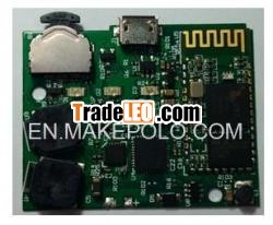
- Attention: Please do not pay before we quote you.The pictureand prices shown are just for exhibition and display of ourproduction .So please send us yourPCB files(Gerber/Protel/CAM/Eagle) for final quotation in email.
If you have anyenquiry,
Pleasecontact:
Smart Tech E Limited
Mrs.Ida
skype: belle-idamail:marketing(at)smartprototype.net
website:www.smartprototype.net
cell:86-15220104899
Business Scope: plastic injection mould making, plastic rapid CNCprototyping , Mockups Making, Laser Molding, Vacuum Casting,Mud-carved Molding, Reverse engineering design and Small batchproduction, PCBA Prototypes, Mechanical Design andreview.
- Detailedspecification of PCB manufacturing:
- Layout: 1-22 layers
- Materials: FR-4, CEM-1,CEM-3, FR4 halogen-free, FR-1, FR-2, aluminum
- Board thickness:0.2-7mm
- Maximum finished boardside: 500*500mm
- Minimum drilled hole size:0.25mm
- Minimum line width: 0.075mm(3mil)
- Minimum line spacing:0.075mm (3mil)
- Surface finish/treatments:HALS/HALS lead-free, chemical tin, chemical gold,
- immersion silver/gold, OSP,gold plating
- Copper thickness:0.5-4.0oz
- Solder mask color:green/black/white/red/blue/yellow
- Inner packing: vacuum,plastic bag
- Outer packing: standardcarton
- Hole tolerance:PTH:±0.076NTPH: ±0.05
- Certificates: UL, ISO9001,ISO14001, RoHS, CQC
- Profiling: punching,routing, V-cut, beveling
- Assembly service providingOEM service to all sorts of printedcircuit board assembly
- Detailed terms forPCB assembly:
- Technical requirement:
- Professionalsurface-mounting and through-hole solderingtechnology
- Various sizes like 1206,0805, 0603 components SMTtechnology
- ICT (In-circuit Test), FCT(Functional Circuit Test)technology
- PCB assembly with UL, CE,FCC, RoHS approvals
- Nitrogen gas reflowsoldering technology for SMT
- High standard SMT andsolder assembly line
- High density interconnectedboard placement technologycapacity
- Quote requirement:
- Gerber file and BOMlist
- Clear pics of PCBA or PCBAsample for us
- Test method for PCBA
- Technical requirement:
Description:
We are also a professionalone-stop R&D engineering service provider, not only we wereformed by a group of people who owned many years of practicalR&D and manufacturing experience, but also we have the resourceof special equipments and instruments for prototype PCBA making ,testing and analyzing, product mechanical-structure prototypeand tooling service, this will be a great help for your R&Ddepartments, and increase the speed and effectivity for your newproduct development. Our service includes Product R&Dprototype engineering service and added-value R&D engineeringservice.
Products change muchmore frequently than before with the competition increasing, if youwant to make your product be unique and attraction, we are the bestparterner for you. We respect customers` technologyauthorization and the technical data will be strictly keptconfidential, our service will be a true-value for you .we locatein Hongkong and Guangdong province , PRC, supported by theconvenient freight transportation express system, we can providethe service to customers around the world.
Product R&D prototypeengineering service includes:
1.PCB Assembly(PCBA) prototype engineeringsample service.
2.RF-circuit Impedence matching service.
3.Tailor-made PCBA Testing Jig sevice.
4.Product mechanical-structure prototype engineering samplingservice.
5.Products & Components sourcing service.
Added-value R&D EngineeringService capacity:
1.Product ID andmechanical structure design / tooling service.
2.Micro-controller circuit design (firmware and hardware ).
3.Universal wireless RF (2.4GHz, 900MHz) remote control circuitdesign.
4.Classic Bluetooth and Bluetooth Low energy (BLE) solution(Bluetooth 4.0).
5.Product ODM(Original Design Manufacturing) service.
(1)PCB Assembly prototypeengineering sample service.
Engineerswith many years of practical experience in PCB circuit design andmanufacturing will give you professional service for your R&Dprototype PCBA sample, and greatly save the timing for productsdevelopment.
(2)RF-circuit Impedence matchingservice.
Professional RF and network analyzing equipments help you to getthe perfect impedance-matching parameters for your RFcircuit.
(3)Tailor-made PCBATesting Jig sevice.
TestingJip is a must tool for batch production of PCBA. We can provide theprofession Tesing Jig tailor-made for your PCBA.
(4)Productmechanical-structure prototype engineering samplingsevice.
Productsmechanical-structure prototype samples are always necessary duringthe products developments stage , we can provide the professionalsevice for this area too.
(5)Products &components sourcing service .
With our rich experience in this field , we can provide sourcingservice for your interested products or electronic components bysmall or large batch in China with goodprice.

