

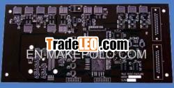
Brand:KDS
Quantity:42000 Negotiable
Send Inquiry
Product Details:
Number of Layers:4-Layer
Surface Finishing:Ni/Au, OSP, HASL lead free, Immersion Tin
Specifications:
- Layers: 2 to 16 Quantity: 42, 000M2/month Surface Treatment: Ni/Au,OSP, HASL lead free, Immersion Tin Material: FR-4, high TG, highCTI or Halogen free etc. as per client request
- Data Inputs- Protel, DXP, Gerber, DXF, DWG, CAM
- Major Laminate- Kingboard, ShengYi and others produce by customer specialrequest
- base Materials- FR4, other materials including High Tg, High CTI,Polyimide, PTFE, Halogen Free by specialrequest
- PCB Maximum board sizeHASL: 546mm x 320mm, OSP: 630mm x 470mm, Ni/Au:570mm x 470mm
- Rigid PCBthickness Single - side to Double side from 0.2mm- 3.0mm
4 layers - 0.4mm - 3.0mm / 6 layers - 0.6mm - 3 .0mm / 8 layers -1.0mm - 3.0mm
10 layers - 1.20mm - 3.0mm /12 layers - 1.40mm - 3.0mm (Small runand Prototype only) - Surface Finishing- HAL /HASL both lead-free and leaded, OSP,Immersion Gold, Immersion Tin
- Copper Foil- from 0.5oz to 6oz, inner layer up to 3oz
- Min. Hole size- 0.20mm, Aspect ratio = 8
- Via holes -Copper PTH, Blind via
- HDI - Class1 for single Blind via
- Impedance controltolerance - +/-10%
- Min. Line Width andSpacing - Max. 0.10mm / 0.10mm (4mil /4mil)
- Solder resist mask- Liquid Photo-Image (LPI), Colours:green, red, blue, black, white, silver grey
- Silkscreen inks– Thermal
- Legendinks: white standard, yellow
- Profiling -Routing, V-cut, Punching, CNC V-cut, Push back
Description:

