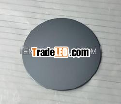
Monocrystalline n type silicon wafer
2016-12-13 18:51 Views:146
Price:Negotiable
Send Inquiry
Description:
Mo
nocrystalline n type silicon wafer
1.FZ-NTD Mono silicon wafer
2.Diameter:50-200mm
3.MOQ:500PCS Mo
nocrystalline n type silicon wafer
| IC grade siliconwafer Product Description |
| | Identifiedas Hi-Tech Enterprise by Henan Science and Technology Agency in2005. PassedISO9001 Quality Management System Certificate in 2005.Developed“FZ-NTD silicon wafer for high voltage silicon rectifier stack andpower transistor” in 2006, this product passed the evaluation byHenan Science and Technology Agency, and was awarded the SecondPrize of Luoyang Technology achievement. Declareda National Invention Patent and a Utility Model Patent in 2009,Utility Model Patent was authorized in October2010. Expanded thescale of production in 2010, purchased land for new factoryplanning and construction.
| | Name | Value | | Brandname | hongtai | | Style | IC gradesilicon wafer | | Model | FZ-NTD | Material | high qualitysilicon ingots | | Surface | lappedwafer | | Diameter | 50-200mm | | Diameter Tolerance | X±0.2mm | | Type/Dopant | N-Type(NTD) | | Orientation | ‹111› /‹100› | | Resistivity(Ω.cm) | 30-1000 | | RRG(%) | N-Type<6% | | Oxygencontent (at cm-3 ) | ≤1×10¹⁶ | | Carboncontent (at cm-3 ) | ≤2×10¹⁶ | | Thicknesstolerance (um) | Accordingto the customer | | Warp(um) | ≤15 oras requirement | | TTV(um) | ≤5 oras requirement | | Place ofOrigin | Luoyang,Henan, China | | MOQ | 500pcs,and trial order accepted | | Usage | Electronicdevice, Discrete device, Integrated Circuit | | Packing | Multilayercarton with polyfoam inner linning | | Paymentterm | 50% TTdeposit | | Remark | OEM&ODM accepted. Customized order accepted | | Delivery time | within onemonth after deposit | | Certification | ISO9001,SGS |
|
|
| IC grade silicon wafer Details show |
|
| Shipping |
- Beijing or Shanghai byair/Qingdao or Shanghai by ship
- Delivery time: within 4 weeksafter deposit.
|
|
| Other hot sellingproduct ranges |
1. FZ-GD lapped wafer 2. CZ Lapped wafer 3. CZ Monosilicon polished wafer 4.FZ Mono silicon polished wafer 5.Silicon Etched wafer |
|
| Inspection |
We do pay attention to thequality of our products. Professional QC group andstrict inspection rules all together gurantee thequality of the products and to win a long term cooperationwith you! |
|
| about US |
| Locatedin Luoyang High-Tech Development Zone, Luoyang HongtaiSemiconductor Co., Ltd isan enterprise which speciallized in manufacturing and marketing ofmonocrystalline silicon wafers, which used for electronic deviceand power component. Ourmajor products include mono silicon lapped wafer, polished wafer,etched wafer etc. |
|
|
| | OurserviceBuyer Guidelines
Choosing Hongtai Semiconductor, you get Top quality, Competitiveprice & Considerate service We expect the long term win-win cooperation with you. Skype: helena51095 Mobile: 0086-18338807239 |
Contact Infomation
Send Inquiry