

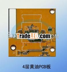
Description:
high thermal conductivity pcb1.ISO14001:2004& ISO9001:2000
2.UL, ROHS, T/S16949
3.short leadtime & best service
4.adopt OEM
Welcometo XingDa Electric Technology Co., Ltd high thermalconductivity pcb maker/manufacturer/ supplier/factory
We canprvide a package of service for all kinds of pcb:
|
1.Specification for PCBManufacture:
Item | Specification |
Numbr of Layer | 1-38Layers |
Material | FR-4, FR2.Taconic, Rogers, CEM-1 CEM-3,ceramic , crockery |
metal-backed Laminate | |
Remarks | High Tg CCL Is Availabe(Tg>=170ºC) |
Finish Board Thickness | 0.2mm-6.00 mm(8mil-126mil) |
Minimun Core Thickness | 0.075mm(3mil) |
Copper Thickness | 1/2 oz min;12 oz max |
Min.Trace Width & Line Spacing | 0.075mm/0.1mm(3mil/4mil) |
Min.Hole Diameter for CNC Driling | 0.1mm(4mil) |
Min.Hole Diameter for punching | 0.9mm(35mil) |
Biggest panel size | 610mm*508mm |
Hole Positon | /-0.075mm(3mil) CNC Driling |
Conductor Width(W) | /-0.05mm(2mil)or |
/-20% of original artwork | |
Hole Diameter(H) | PTH L: /-0.075mm(3mil) |
Non-PTH L: /-0.05mm(2mil) | |
Outline Tolerance | /-0.125mm(5mil) CNC Routing |
/-0.15mm(6mil) by Punching | |
Warp & Twist | 0.70% |
Insulation Resistance | 10Kohm-20Mohm |
Conductivity | <50ohm |
Test Voltage | 10-300V |
Panel Size | 110×100mm(min) |
660×600mm(max) | |
Layer-layer misregistration | 4 layers:0.15mm(6mil)max |
6 layers:0.25mm(10mil)max | |
Min.spacing between hole edge to circuity pqttern of an innerlayer | 0.25mm(10mil) |
Min.spacing between board oulineto circuitry pattern of an innerlayer | 0.25mm(10mil) |
Board thickness tolerance | 4 layers: /-0.13mm(5mil) |
6 layers: /-0.15mm(6mil) | |
Impedance Control | /-10% |
Different Impendance | -/10% |
2. Details oftech:
PCB/ PCBATechnic
1).Professional surfacemounting and through hole soldering technology;
2).Various sizes, like 1206,0805, 0603 components SMT technology;
3).ICT(In Circuit Test),FCT(Functional Circuit Test) technology;
4).Nitrogen gas reflowsoldering technology for SMT;
5).High standard SMT&SolderAssembly line;
6).High density interconnectedboard placement technology capacity.
PCB/ PCBA Quoterequirement
1).The detailed files(Gerber file/ PADS/ AutoCAD/Protell/ Power PCB/ DWG/ schematicetc and BOM);
2).Clear pictures of PCBAor samples for us;
3.View ofXinDaXing:
1) PCBAFactory
2) PCBfactory
3) PCB/ PCBA Testcorner
4. Whyus?
Quality
Our UL/Rohsstandards garantee our quality from startto finish. Whether it''s a simple custom product or acomplex production run, XingDa will adhere to thehighest quality standards.
Capabilities
XingDa offers thelatest and best capabilities andqualifications ensuring highest quality in eachpiece of product we produce.
Experience
We have been specializing in PCBand PCBA industry for many years. Our management and engineeringteam possess over 10years combined PCB and PCBAexperience, so does our sourcing team.
Protecting yourinterests
Protecting your IntellectualProperty comes first! All your files/ information regarding designof your products will only be used for your projects, will never beleaked out.
Price and leadtime
We will offer the best price andshortest leadtime for your PCB and PCBA since wehave professional engineering department, sourcing departmentand producing department etc.
5. Delivery andPayment:
1. By DHL, UPS, FedEx, TNT etc.
2. By EMS (Usually for Russia Clients), price is high.
3. By sea for mass quantity according to customer''s requirement.
4. By customer''s Forwarder
5. payment prefer -- T/T, Western Union ( HSBC )
If any need or questions, pleasefeel free to contact me any time. You can send me email orinquiry via Alibaba. Thank you.

