

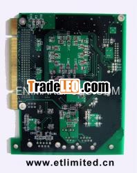
• PCB fabrication, componentssourcing, DIP/SMT/BGA assembly, plastic shell boxproduction.
• High precision 0201,0402,0603,fine pitchQFP,BGA, bonding size components.
• High quality 1-12 layer blankPCB .
• The base material can be FR4,high TG, F4BK, Aluminium, Ceramic, CEM-1/22F and other specialmaterials.
• Surface finish: Lead freeHASL,OSP,ENIG,Immersion silver.
• Electrical test,open/shorttest,impedance test,Solderability test etc.
• Other technology: Goldfinger,peelable mask.blind and buried hole.
•The boards can be sent byDHL, UPS,FEDEX, EMS,TNT etc to save the delivery time.
Whychoose ET Limited?
• 15 years solidPCB manufacturing experience.
•PCB→PCBA→
• Your anyrequirements will be met and give you a best relativesolution.
• We always try our best to helpour customer to Keep allcosts to minimum and maximize our customers''benefits.
• Goodafter-sell service !Any quality problem happened in ourPCBA will be solved at the most prompt time. wealways provide free-repairment service. All your inquiries will bereplied within 24 hours.
Products experienceapplication range
industrial, automotive, medical, computing,storage,instrumentation, traffic, industrial power, battery,firealarm,CCTV, wireless communication,telecommunication, networking,printer and house controller.
ManufacturingCapability
| Item | Standard | High-endproduct |
| Layer | 2-12 Layer | 14-18 Layer |
| Maximum boardthickness | 5.00mm | 6.00mm |
| Minimum board thickness(4layers) | 0.4mm | 0.38mm |
| Minimum board thickness(2layers) | 0.3mm | 0.25mm |
| Minimum corethickness | 0.10mm(not include copper) | 0.05mm(not include copper) |
| Largest PanelSize | 457.2 X 609.6mm | 533.4 X 609.6 mm |
| Thinnest PPthickness | 0.05mm | 0.051mm |
| Maximum inner layer copperthickness | 2.0 oz | 3.0 oz |
| Minimum inner layer copperthickness | 0.5 oz | 0.3 oz |
| Maximum outer layer copperthickness | 2.0 oz | 5.0 oz |
| Minimum outer layer copperthickness | 0.5 oz | 0.3 oz |
| Mini linetrace | 3MIL/3MIL | |
| Mini finished holeaperture | 4MIL | |
| Aspect ratio | 7:01 | |
| Mini SMD space | 12MIL | |
| Mini SMD test space | 10MIL | |
| Layer to layerExcursion | 3MIL | |
| Solder mask contrapositiontolerance | 3MIL | |
| Optics anchor pointtolerance | ±1MIL | |
| Finished board level | ±5MIL PERINCH | |
| Max finished boardsize | 20"*24" | |
| Mini board thickness | 4LAYERS:16MIL | |
| 6LAYERS:24MIL | ||
| 8LAYERS:32MIL | ||
| Aperture tolerance | PTH±3MIL,NPTH±1MIL | |
| Hole tolerance | ±2MIL | |
| Impedance control | 75,65,50 OHM /-10% | |
| Usual copperthickness | 0.5 oz – 2oz | |
| layer | 2~10LAYERS | |
| Line QTY betweenholes | 3 LINE/CHANNEL | |
| Plating Gold finger | NI/AU 150U"/10~20U" | |
| Complete Plating Goldfinger | NI/AU 100 U"/5~20 U " | |
| Complete immersiongold | NI/AU 100U"/3~5 U " | |
Factory View and WorkshopView
ET Limited, the best manufacturer to test andrealize your PCB circuit design.
Please try us! You will find that we arethe right PCB and PCBA supplier youwant.

