2.pemtron spi
3.pcb inspection
4.3d solder paste inspection
5.solder paste height
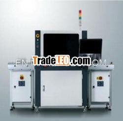
Inline spi solder paste inspection optical inspectionsystem
ProductFeatures:
1.The use of PSLM combined with the PMP to achieve 100%high-precision solder
paste 3D measurement in SMT productionline.
2.Using PSLM technology, changed the traditional way ofgenerating struct light,
the traditional glass grating moire (Moiré) requiresmechanically driven by a
piezoelectric motor (PZT). By using PSLM, no need glassgrating and mechanical
parts any more. The elimination of the mechanical drive andmoving parts,
greatly improving the ease of use and avoid mechanical wearand reduce
maintenance costs.
3.Megapixels of ultra-high frame rates and high dynamic rangeindustrial cameras,
with the high precision grade balls-crew and guide railmechanical structure,
realizing high-speed and stablemeasurement.
4.Patented 3D DL (Diffuse lighting) technology, combined with2D RGB light source
achieve easy to use. It is perfect solution to solve theshadow effect and reduce
noise interference in 3D measurement.
5.Gerber data conversion and import, achieve automaticdetection of the entire
board. Manual “Teach” function realize user-friendlyprogramming and test job
generation in case of no Gerber datasituation.
6.The maximum detectable height increased from the traditional ±350um to
±1200um, not only can detect solder paste, also applies tothe detection of
opaque objects such as red glue and black epoxy and othernone transparent
object.
7.Friendly and simple user interface, five minutes ofprogramming and one key
operation.
8.Powerful “Statistical Process Control (SPC)”, provide a plenty oftools, user-
friendly real-time monitoring of production, reduce defectscaused by poor solder
paste printing and improve customer productquality.
9.PCB size up to 480 × 450mm, can be widely used in themanufacturing of
electronic products, the application range like: mobilephones, digital products,
television, audio and video appliances, computer accessories,automotive
electronics, medical electronics, LED, etc.
Measurement Principle | 3D white light PSLM PMP |
Check the project | Volume, area, height, position, shape, XY |
Bad type | More / less tin, solder paste stencil, sharp pull, bridging,offset, special-shaped, dirt etc. |
FOV size | 48 * 34 mm |
Accuracy | XY: 10 um, height: 1 um |
Repeatability | Height: < 1um (4 sigma), Volume: < 1% (5 sigma) |
Test speed | 2300 mm² /FOV |
Mark-point detection time | 1 second/1 pc |
Max Measurement Height | /-350 um, ( /- 1200 um, option) |
PCB maximum bending | /- 5 mm |
Min pad spacing | 100 um |
Min test size | Rectangle: 150 um, Circle: 200 um |
Max PCB size | 510 * 505 mm |
Engineering Statistics | Histogram; Xbar-R Chart; Xbar-S Chart; CP&CPK; %GageRepeatability data; SPI daily/weekly/monthly reports |
Read position detection | Gerber Format(274x,274d),Teach |
OS | Windows XP professional or Windows 7 professional |
Dimension and weight | 1000 * 1000*1530 mm, 865 kg |

