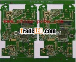
Brand:H.C.C
6 Layers Printed Circuit Board most of our products comply withthe ROHS Directive ,and we have a acceptance of nearly 100
Items | Craft Ability | |
1 | Surface Finish | HASL,Immersion Gold,Flash Gold,Gold Plating,OSP,Immersion Tinetc. |
2 | Layers | 2-30 layers |
3 | Minimum Line width | 3mil |
4 | Minimum Line space | 3mil |
5 | Min space between pad to pad | 3mil |
6 | Minimum hole diameter | 0.10 mm |
7 | Min bonding pad diameter | 10mil |
8 | Max proportion of drilling hole and board thickness | 1:12.5 |
9 | Max size of finish boar | 23inch*35inch |
10 | Rang of finish baords Thick | 0.21-7.0mm |
11 | Minimun thickness of soldermask
| 10um
|
12 | Soldermask
| Green,Yellow,Black,Blue,White,Red,transparentphotosensitive,,soldermask,Strippable soldermask |
13 | Minimum linewidth of Idents | 4mil |
14 | Min Height of Idents | 25mil |
15 | Color of silk-screen | White,Yellow,Black |
16 | Date file format | GERBER FILE and DRILLING FILE, PROTEL SERIES, PADS2000 SERIES,Powerpcb SERIES, ODB |
17 | E-Testing | 100% E-TestingHigh Voltage Testing |
18 | Material for PCB | High Tg MaterialHigh FrequenceROGERS ,TEFLON ,TAConIC ,ARLON)Halogen-free Material |
19 | Other test
| Impedance,,Testing,Resistance,,Testing, Microsection etc.,
|
20 | Special technological requirement | Blind & Buried Vias and High Thickness copper |

